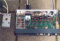
A collection of NRD-515 oriented diagrams and modifications
Drawings are NOW in 2-colour BW 600 DPI TIFF format with LZW or G4 compression.
They are very hi-res inside the PDF's
Latest change: Highres TIFF removed due to lack of provider storage
Only in PDF will do.......
By unilaterally canceling my Microsoft Live subscription and thus hosting my server name DNS pe1abr.homeserver.com to the current IP number and then also a modem change with associated IP change, my (site) storage server has been made inaccessible. Thanks everyone! I have taken out a replacement DNS service through my router manufacturer, called pe1abr.tplinkdns.com. If you have saved old links to the server, please replace the DNS provider part in that link. Happy downloading!
SHAME/pillory/scandal: April/May-2017, virus uploader on my FTP server:
This person was trying to fuck-up the upload folder on my PE1ABR server
With analyser software I found a whole list of them, they all act in the same way!
IP Address
Country
Region
Street, City
37.55.94.231
Ukraine
Kharkivs'ka Oblast
Molochna St., Kharkiv / Charkov
Links to original
NRD-515 drawings:
Item (All 2 colour 300 or 600 DPI High Res TIF files)
Highres TIF in PDF file
Principal working overview diagram
Appendix 1
Main chassis and Front Board circuit diagram
Appendix 2
Rx board circuit diagram
Appendix 3
Synthesizer board diagram
Appendix 4
Power supply - voltage distribution between IC's
Appendix 5
Power Supply regulator board
Appendix 6
Anti mains rattle feedthrough possible from the rectifiers on regulator board.
Adding extra capacitors on the AC side of the rectifiers to cancel this. Modified version Appendix 6.
The bridge rectifiers get so hot that you can burn your finger on it. You could say that they are constantly trying to desolder themselves. I mounted
mini heatsinks on them.
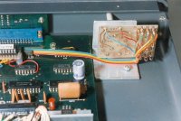
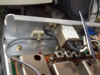
Safety modifications mains filter to comply with new EMC regulations. IEC power input exchange with real mains-inlet filter. Also reduces radiation on VHF-I (TV) band. Click on IE icon to see a sub page with mains-inlet pictures.
Also added a picture of a too low creep distance and mains/lightning overvoltage flash-over.
Result: dozens of IC's blown.
A PDF version of the CPA-94 main tuning dial encoder board.
Thanks to cooperation with PA0A (Ex: PA0AWN) who did the research.
A number of times (in several 515 devices) I have had to replace the output IC (a 4011) in the CPA-94 unit because it broke "just like that" without any reason. Sometimes the shaft bearings also changed places to move play. Nowadays the bearings can be ordered from AliExpress. - originally it was the MS126ZZ - but the MF126FF (the flanged version) is better suited.
A PDF made from a scan of the CPA-33 diagram, this one is used a.o. in the NRD-75. The internal circuit is identical to the CPA-94, I got it from Japan, from Ken.
A PDF version of the CGA-68 main (triple) VCO unit for the NRD-515. If something goes wrong, a 10 MHz range mutes ( 0 - 10, 10 - 20 or 20 - 30)
A PDF version of the CGA-94, the JST-100 triple VCO unit.
Compare this with the above CGA-68, the CGA-68 decoupling has been improved.
A redesigned PDF version of the original JRC 455 kHz filter board.
It is meant as a replacement of the original board and for the same filter types.
Due to public demand I made my own layout. The PCB "fingers" connected for possible electroplating. Meant to etch your own filterboard!!
Also a 4x version on one A4 sheet. Cut this sheet into 2 parts and tape them together for a double layer 1/2 A4 for 2 PCBs. Better blackening!
multi-PCB
A redesigned PDF version of the ESKA 455 kHz filter board.
This board is for high quality ceramic filters, NO Xtal types. It can hold all the Murata filter variations in metal enclosure. It will NOT fit plastic SFR or CFW types, use an extra mini mounting board from one of the next items.
A Kokusai is still possible. NO transformers, only LC and CL networks. Added is a DC separation Cap, adviced by Murata! NO DC to ground on the output.
Due to public demand I made my own layout. Meant to etch your own filterboard!!
Please keep in mind to use the proposed screened coil caps or coil forms!!! Or use small 4A11 toroids in 90 degree position to each other! The circuit is very sensitive to HF leakage!
A once more redesigned PDF version of the ESKA 455 kHz filter board.
This board is almost the same as the previous.
I found a flaw in the ESKA schematic. The low Q DC bypass inductance is switched in parallel of the LC circuit. Its parasitic damping and capacitance is in parallel with this circuit. I found this wrong and changed the diagram and the PCB layout once more
Put the previous PDF in a second tab and compare to see the differences.
A small add-on board for the above two filter boards. It can hold two ceramic SFR or CFW types in cascade, in this version without Z conversion with L-C circuits, a plug-in for in a Kokusai position / footprint. No -60 dB far suppression, but near -100 dB (or more) is possible!
Meant to etch your own filterboard!!
Added a multi print PCB sheet, made with additional postscript code.
multi-PCB
Two more (different) very small add-on boards to hold two cascaded SFR or CFW455 type filters.
The footprint in these versions is equal to the bigger "metal" Murata filters.
Some more details how to convert the Z (impedance) of an 455 kHz IF filter to a different Z value with L-C or even C-L networks. If you combine them, first LOW-pass then HIGH-pass you even better suppress false stop-band effects.
Some sites with "calculation engines" are these:
in the PDF's right some results that are near, but NOT EQUAL to the existing values used in the NRD-series.
In the next item you read that JRC adjusted the Cap-value. (The motherbord Z is also not equal between 515-525). The mutual leak-effect is also reduced with different mounting - one L laying down and one L standing up in the NRD-525.
Keep in mind!:
The two motherboad filters are Z transfered from 1K on board to the filter Z. For the 6 kHz AM filter this is 2K. So L-C for 1K to 2K. The Kokusai SSB filter is not equal transferred on in- and output! See test PDFs further down.
The big X-tal position on the add-on PCB is adjusted 2x to 600 Ohm (on motherboard), the narrow Kokusai can be anything with the transformers.
Now look at the LC values in both PDFs right.
Also: the filter ground is NOT connected to frame ground. There needs to be a DC bypass from filter I/O to filter GND, otherwise the switch diodes won't work.
Analog
Toroids
An add-on board with the same footprint as the bigger NDK Xtal filter units.
It is meant to hold two good and selected SFR or CFW filters in cascade. The Z is adjusted with two LC circuits, as above:
Use 2 small 10 - 14 mm 4A11 toroids in 90 degree position to each other! The circuit is very sensitive to HF leakage! Also wind a shim of copper foil around the plastic filters (in S-curl) and connect to the top earth/ground copper layer = to the wire in the middle connected to the NDK Xtal mounting holes. The top-copper is NOT connected to filter ground. So it is needed to place one earth wire through both the NDK bolt holes.
Use 30 - 33 windings (measure!) on a 13 mm (TN13/7.5/5) 4A11 toroid (or FT50-43), average AL = 360, to make 330uH and C= 220 pF (used in NRD-515). After simulating the incircuit f-res, probably 270pF is more accurate for 455 kHz (used in NRD-525 and NRD-535)
Using 2x a 330uH toroid as proposed gives 20 - 30 dB improvement with the standard AM 6kHz CLF-D6S. Also in NRD-525 and NRD-535.
Instead of 2x an LC circuit, it is also possible (perhaps even better) to do the Z-conversion with a mini toroidal transformer, as described on this page for the Kenwood CW filter in the NRD-515. In the NRD-515 non motherboard (and 525 + 535) the circuit-Z is 600 Ohm. On the 515 motherboard 1 KOhm is used. In other Rx sometimes between 1K Ohm and 2K. (The Kenwood CW filter used was 2K). With a transformer this is easier to cope with and less leakage. Ground separation easy possible by cutting ground traces, otherwise the switch diodes won't work. Filter ground is NOT frame ground.
The pass-band may have some (ripple) bumps, but the shoulders are very steep (shape factor under 1.5 ) and superior far suppression (stop band attenuation).
With postscript/EPS manual edit I used some postscript engineering tricks and created a multi (6x) PCB version
PCB
test SFR455H
test CFW455IT
multi PCB
A slow homeserver http link to the ESKA Option 1+2 instruction manual for the NRD-515. The pages have been higly edited and reworked to make them perfectly readable.
All converted to 600DPI, with pure black-white G3 TIFF's, size about 9 MB
I also tried to clone the PCB design of option 2 without ever seen it. I only had a mediocre scan of the diagram, improved in the above item.
In the PDF you see how far I got with this cloned version of the design.
A slow homeserver http link to the complete NRD-515 instruction manual. With all the A3 diagrams inclusive!! All 600DPI, size about 5 MB
A slow homeserver http link to a complete reworked NRD-515 service manual.
Also with all my A3 600 DPI diagrams inclusive!!
The original scans are in 400 DPI, but they are all hacked, cropped, cleaned/stuffed and edited by me. And with some additions. More than 100 pages!
More than 35 annoying typos graphically removed.
Links to original
NDH-518 drawings:
Item
Highres TIF in PDF file
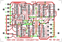
Memory Unit NDH-518 circuit diagram (made from 600DPI TIFF-G4)
Modified memory unit diagram (for the options/modifications further below) made from TIFF-G4
Complete scanned NDH-518 Memory unit instruction manual With A3 diagram inclusive
Complete scanned original NDH518 Service Manual, scanned not in the most ideal settings according to the latest standards, but this is all that is available!!!
Thanks to Mike - VK4GV
Mike - VK4GV also pointed me on the memory card in a plastic sheet that was with the memory. Hell, I just forgot to add it to this page!
Here you find a highres 600DPI black and white scan that you preferably print on yellowish 200 grams heavy card-paper. Yes, it was yellow, see the second scan in color. But preferably print the BW version on yellow paper. Its a lot smaller in kilobytes and even sharper.
BW
Y
Complete NDH518 Service Manual, not the same as above, but a completely reworked version. Hardly readable 256 color gray datasheets in only 100 DPI replaced with my own scans from NEC book.
Bi-lineair pixel enlargement, histogram push and conversion to 2-color TIFF-G4 in 300 DPI for those pages that cannot be replaced.
Circuit diagram replaced with own A3 600 DPI scan. Overview diagram replaced with scan from users manual. Added a page with memory test info.
And take a look at the front page.
Much more info, due to lossless 2 color compression 4x smaller than above!
Links to NRD-515 test reports and other documentation sent to me as a gift...
Item - colored text in a second language
PDF
JRC NRD-515 test report in German language from the magazine "Beam", February 1982 edition
JRC NRD-515 Testbericht in deutscher Sprache mit technischen Daten aus der Zeitschrift "Beam", Ausgabe Februar 1982
JRC NRD-515 test in German language, extract from the magazine "Weltweit Hören", December 1980 edition
JRC NRD-515 Testbericht in deutscher Sprache mit technischen Daten, Exzerpt aus der Zeitschrift "Weltweit Hören", Ausgabe Dezember 1980
JRC NRD-515 test in German language from "Kurzwellenempfänger - Die Qual der Wahl" by Rainer Lichte, 6th edition from 1984, an equivalent English phrase for the booktitle would be: "Shortwave receivers - The Agony of Choice"
JRC NRD-515 Testbericht in deutscher Sprache mit technischen Daten aus "Kurzwellenempfänger - Die Qual der Wahl" von Rainer Lichte, 6. ausgabe 1984 (gleicher Inhalt wie in der Zeitschrift "Weltweit Hören", Ausgabe Dezember 1980)
Some pages with a NRD-515 (plus Gilfer version) review from the 1982 edition of the WRTH
TIFF processing complete!
The advertisement with the NRD-515 from the 1982 edition of the WRTH
The image is very reduced to 2-color to reduce kilobytes (15 times smaller), but will print pretty OK.
It has a clumsy mistake, do you see a small picture version of the NSD-515 transmitter? NO, it is also the Rx!
An earlier advertisement version with the NRD-515 (almost the same as above) with the previous version of the memory unit: NDH-515. Here the transmitter NSD-515 has the correct image!
This version is in color!
Original NRD-515 German language user manual from Richter & Co., Hannover
Original NRD-515 deutschsprachige Bedienungsanleitung von Richter & Co., Hannover
JRC NRD-515 review report by Kirk Allen and David Clark from Fine Tuning's Proceedings publications.
This is NOT the same version as on other sites on the web, this version is brushed, stuffed and cleaned.
I also replaced the images with better scanned (identical) versions!
Only for the German (Richter ?) version, simple reverse engineering sketch of a strange add-on PCB that blocks Rx under 146 kHz. The identification name on the board is "NRD-515 RFK", RFK probably means RicoFunk?
Nur für die deutsche Version (Vertrieb Richter & Co.?) :
Die deutsche Version (vielleicht nur die welche über Richter & Co. vertrieben wurden mit FTZ-Nummer?) hat einen eingeschränkten Empfangsbereich. Empfang unter 146 kHz ist nicht möglich, das Gerät wird "stumm". Hier das "Reverse Engineering" des PCB und der Beschränkungs-Schaltung. Simple PDF-Skizzen.
Diese Schaltung kann relativ einfach entfernt werden! Im "Beam" Artikel oben ist diese zusätzliche Schaltung in der Nähe des Abstimm-Encoders zu sehen. Identifikation ist "NRD-515 RFK", RFK bedeutet vielleicht RicoFunk?
Original SUMICON/HIROSE 1600 series connector PDF, plugs widely used in JRC equipment! I also made a small TXT list with order info about those connectors. Click connector icon right or HERE to see that list.
In this link the Hirose Europe site with some resellers.
Bernard Malet sent me a document with his search for replacement VHF transformers, widely used in the NRD-515 in the 65 - 71 MHz circuits.
They do not seem to exist anymore and were specially made for JRC by SUMIDA.
In this PDF document a method to wind them yourself on similar VHF cores from TOKO. At a former local electronics shop (discontinued Kent Electronics) I myself have found similar TOKO VHF transformers that could also be usable. Maybe even without rewinding, if needed, only adding a secondary winding.
Click image right to see my own replacement document.
The PDF icon is the document from Bernard.
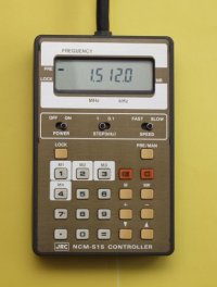
Click over here for a scanned NCM-515 manual. Made with an Acro-7 scan plugin, but compatible with Acro 5 and above. I've added the very hard to obtain diagram of the connector box CQE-515 as last page.
Also read my Addendum for the NCM-515 manual
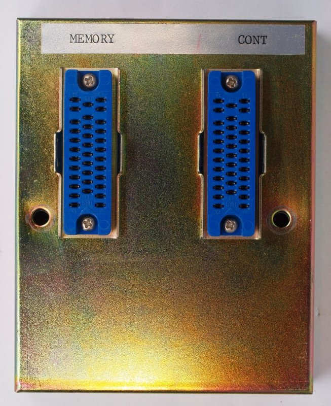
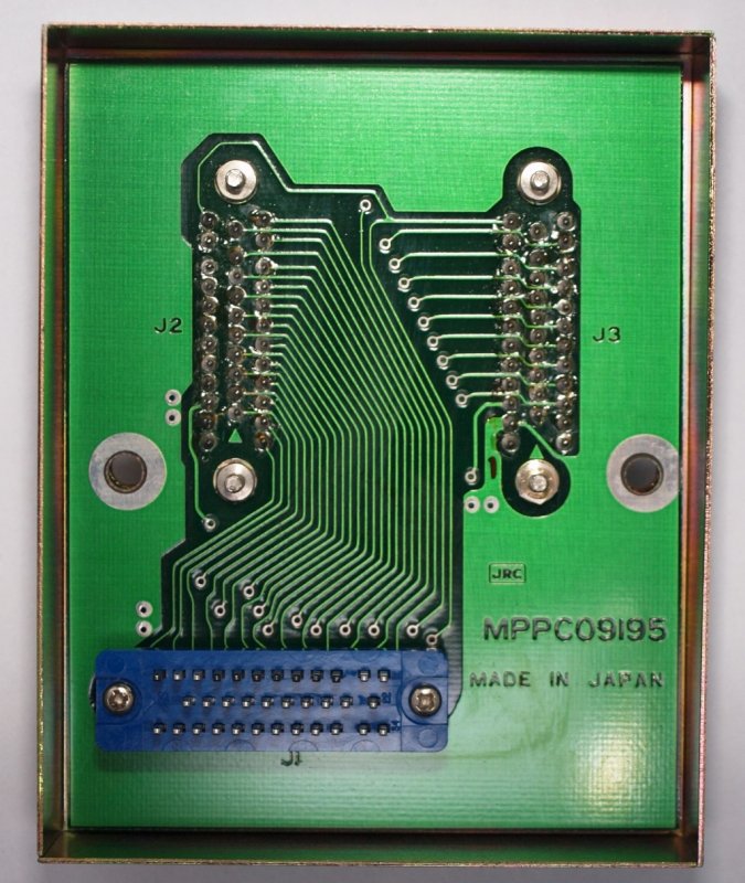
I tried to re-design the board inside the CQE-515 unit, see PDF
CQE-515
CQE-515
Click over HERE for lots of PDF files about hardware used in the NRD-515 and in my designs.
And now some links to my modification drawings and designs
Almost all the drawings are made available in PDF format.
You MUST have Adobe Acrobat reader installed, see at the bottom of this page. I try to keep PDF's compatible as low as AR version 5, some even AR3 ! If problems: copy PDF files to harddisk first without double click, but with "copy to"
A very simple method to Backup the Synthesizer:
PDF with synthesizer backup circuit to retain the "VFO" contents during power off.
Basically the same circuit as if 3 to 4 NiCd cell's were used...., but now with a turbo capacitor connected to TP35, although in early versions TP35 is not there.....
If you can't find TP35, where should it be on the drawing?
And where on the board?
It is wise NOT to connect +5 and GND to the synth board, but directly to the power supply board connections. So only one wire to synth PCB.
The first version of the backup with an early turbo capacitor
BFO control only for BFO/BC-tune button with Auto BC Tune (v1.1):
The BC-TUNE tuning can be automated!
The tuning voltage is exactly measured at some intervals and that information is calculated to the whole range and put into an EPROM.
A new Visual Basic utility to convert the measured info to EPROM data is available now!
A D/A converter makes tuning voltage of the EPROM data again. More easy BC tuning and the BFO tuning now also works for DX zero tune on the BC band.
A very small portion of hand-tune is still available to check the auto tune.
The original version used a cheap Ferranti D/A chip that is hardly available nowadays.
EnglishDutch Diagram BC-Tune D/A converter and amplifier
PDF with BC-tune PCB layout - both sides ZIP file with example eprom file + QuickBasic 4.5 eprom creation programs - comments in DUTCH
The first version of the backup with an early turbo capacitor and also the first version BC-Tune, with the old Ferranti D/A chip
A new version 2.0 of the Auto BC Tune with more recent DA-converter: (And a NEW VB6 conversion shell)
EnglishDutch Diagram BC-Tune D/A converter and amplifier
new BC-tune PCB layout - both sides
New ZIP file with example eprom file + NEW Visual basic 6 EPROM creation program - And a part of the program listing from VB6 - comments in DUTCH, with simple English Notepad HELP file. Diagnostic output with over 1000 lines of calculation results. Due to this list with tune info some minor roundup bugs removed.
If your XP or W2K is very "clean" you also need the VB6 RUNTIME and dialog files. It is still possible to run it under W10, but with some effort to register the above runtime libraries as admin.
Memory Modifications
Only a limited number of memory channels were originally used. From 1x 24 in the earlier NDH-515 to 4x 24 in the NDH-518. There are many more channels available, e.g. 256! Here some tricks to address them in binary mode and convert the display view back to decimal (in BCD mode). Eventually you get (max.) 8x 32 or 4x 64 channels! If you change as less as possible on the outside of a NDH-518, only one switch will double the available channels from 4x 24 to 8x 24.
Or for the NDH-515 with an extra (rotary) bankswitch from 1x24 to 8x 24! In the inside mostly a chip for coding from BCD to binary and a second chip back from binary to BCD (for the correct display view) is always needed. This could be with a GAL array or an EPROM or both.
To address them all in an easy way also an additional UP/DOWN counter board was designed. But a more simple version with extra bank-switches is also possible.
The Up-Down PCB
Modifications executed on a NDH-515 memory unit:
This is the least complex version, only an 8 channel bankswitch is added and of course the binary encoding and binary-BCD decoding chip. This will give 8x 24 channels in place of the original 1x 24.
If you look at the neat way it is added you wonder why JRC didn't do it this way.
PDF with the old original 1984 binary coded decimal matrix switchboard PCB layout as can be seen on the pictures PDF with binary coded decimal add-on universal (new 1994) switch board for NDH-515 ZIP file with Gal array decoders - EQN and JED files
Circuit diagrams are for a slightly (minor) different GAL version as NDH-518 PDF with circuit diagram GAL expansion for NDH-515 memory unit
Off-topic PDF with a further development of the 1984 board. Here a 2716 or 2732 is used for the code table. The table can be modified without a soldering iron.
Sub page with some pictures
UP/DOWN counter control for a NDH-518:
To address all channels in an easy way an additional UP/DOWN counter board was designed. The rotary 24 position switch has been replaced with a miniature DIY made opto encoder. Like the tune dial! A Bourns potentiometer sized contact interrupter is also possible.
PDF with up/down countercontrol add-on board PCB CAD PDF with circuit diagram binary UP/DOWN counter control PDF with binary to BCD decoding for displays with eprom - 64 channels p/bank PDF with binary to BCD decoding for displays with GAL - 32 channels p/bank Zip file with GAL related JED and EQN files for new 32 channel GAL version
64 and 32 channel decoding chips can also be used for the (above) 24 channel rotary bankswitch version
Sub page with some pictures
Accessibility modification on a NDH-518 unit to make it into a remote controllable memory:
This is the MOST complex version, NOT advised to start with!! PDF with circuit diagram part 1of 5 for memory accessibility options
(Memory control and read-out mod)
PDF with circuit diagram part 2 of 5 for memory accessibility options
(Up-Down control board with some additions for remote control)
PDF with circuit diagram part 3 of 5 for memory accessibility options
(Internal connections between sub-boards)
PDF with circuit diagram part 4 of 5 for memory accessibility options
(I/O buffer board and I/O connector wiring to external controlbox switches)
PDF with circuit diagram part 5 of 5 for memory accessibility options
(The channel control part of the external control box)
PDF with PCB CAD layout for memory accessibility options inside the NDH-518 PDF with PCB CAD layout control box for memory accessibility options PDF with PCB CAD layout Up/down countercontrol add-on board PDF with front panel example control box for memory accessibility options Zip file with GAL related JED and EQN files for new 32 channel GAL version
(same GAL-chip and up/down CAD board version as NDH-518 above)
Sub page with some pictures
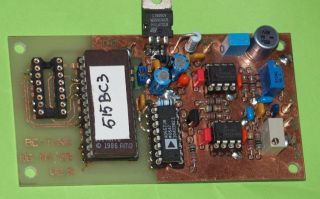
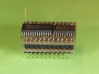
A DIY SMD module to replace blown 5101 CMOS RAM in the JRC memory unit
At one time I got hold of a scrap NRD-515 with lightning damage.
The repair was successful, more than 25 IC's were blown!
But the NDH memory unit remained a problem,
the memory IC's were nowhere available at that time.
I then designed my own replacement module, it works great!
Page with all the info to build it LINK No need to build it anymore?
As a replacement, the Signetics version PCD5101 is now for sale at AliExpress, see search link
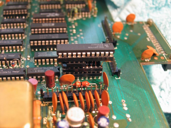
Also a blown uPB426 (PROM) chip on the synth board ??
This chip is the band segment decoding table (PROM) out of the frequency range
Click to go to the page with PDF hardware information and how to build your own decoding chip with a GAL22V10!!
It took some effort, but works fine
Too bassy sound?
Early versions of the NRD-515 rev A and rev B had a bright, but somewhat distorted sound.
Revision C had the bassy sound, for most people a little too bassy.
It all has to do with the value of capacitor C333 (near TP-28), which is part of a low-pass network. In rev-B I've seen the value of 1 nF, which is wrong.
In rev-C I've seen a value of 33 nF ( = 0.033 uF) which is just a little too high.
The one and only correct value for the most perfect sound experience = 22 nF = 0.022 uF.
If you change this capacitor C333, it is wise to change another cap C330, the one for side-tone IN. It does NOT change anything to the side-tone IN sound, but now you can (mis-) use this input for an external FM or ECSS-AM decoder.
I have used a value of 0.56 uF which was available.
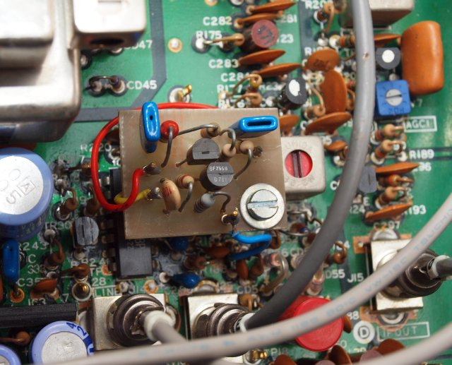
AM detector buffer:
The single diode AM detector causes a too high a-symmetric load on the last IF stage.
With a small buffer with low Z-out the distortion is gone, also audible as cleaner SSB!!
After the build-in of the buffer:
Max. 455 RF level must be lowered and re-adjusted with RV7, checked on TP17.
Due to the reduction of LC damping the level goes up a lot and could give distortion.
My setting is max. 5V peak-peak with heavy modulation on TP17.
The service manual uses a generator with a low level of 30% modulation and a RF level of about 0.8V RMS on TP17 = equal to 2.3 V peak-peak.
So not much difference.......
PDF with drawing of an AM detector buffer PDF with layout of an AM detector buffer
Alternative CW crystal filter:
JRC's narrow CW crystal filters are very hard to get nowadays and are too expensive.
And there is something very wrong with it!
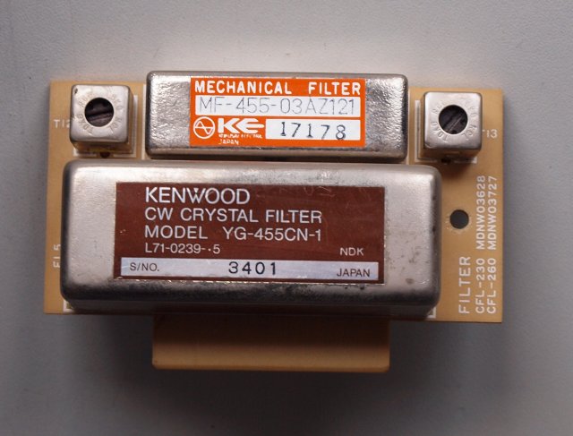
Kenwood has equivalent 250 Hz - 455kHz filters, in the same footprint type YG-455CN-1, also from the same NDK factory.
They won't work as it should because the wrong higher impedance and a DC short circuit to ground.
But with two small impedance transfer and DC separation toroids it will work,
even much, much better than the original JRC 300Hz CW-filter, which has a VERY, VERY bad shape factor (above 4) !! See further down.......
The toroids you see are 3E25 - 14mm - AL=2200 It transfers the 600 Ohm to 2000 Ohms and back. It also gives the needed DC separation. Windings are 20 for 600 side and 36 for 2000 side. So it's about 1 to 1.826 in N, and 1 to 3.333 in Z.
A smaller 10 mm 3F3 toroid is even better. Less losses. (recently available via TME-Poland)
10mm 3F3 toroid AL=740, windings in this case 34 for 600 and 62 for 2000 Ohm side.
Thick (5mm) 12.5 mm 3F3 toroid AL=900, N1= 31 and N2=56. And this is one compatible with FT50-77
Fine KENWOOD YG-455CN-1 and 600 Hz KOKUSAI (in red)
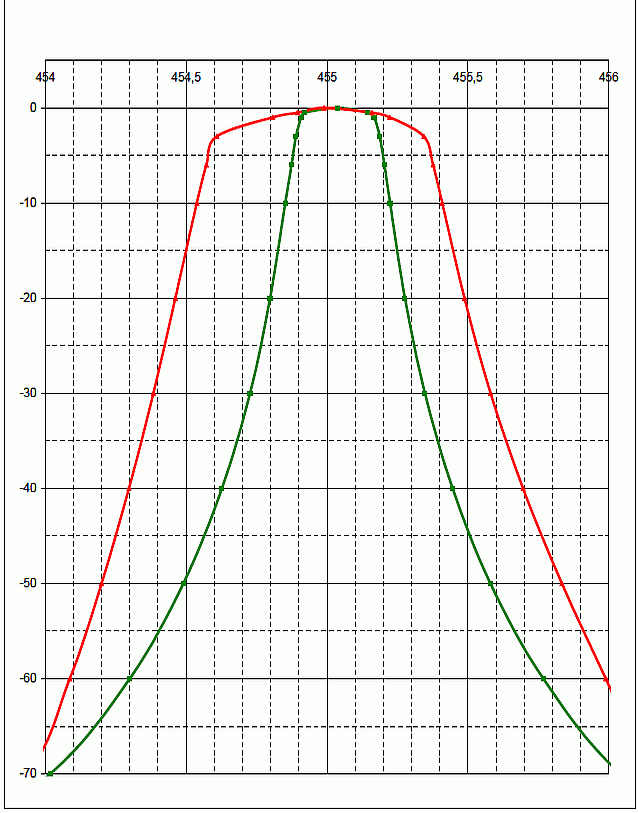
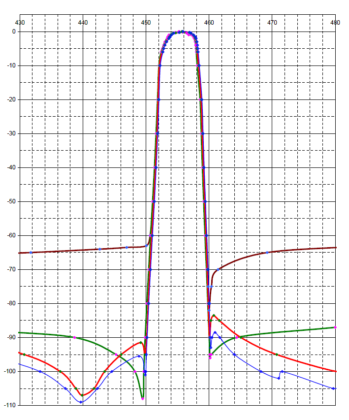
CW FILTER COMPARE..... (A very, very bad shape)
You see the curve shape of two tested CW filters
on two different filterboard's.
The small curves images left and right can be enlarged.
The RED curve on both is a 600 Hz KOKUSAI.
The smaller GREEN curve left is the perfect KENWOOD
narrow CW filter YG-455CN-1, made by NDK.
Measurement data:
-6dB =293Hz | -60dB =471Hz | shape =1.61
loss =4dB. Two additional toroid transformers are needed, see previous item on this page.
At right you see the (GREEN) JRC CW filter YF455DPB curve. Also known with a JRC code as CFL-230. It is rather wide-legged and JRC should have ordered a better filter at the NDK factory.
Measurement data:
-6dB =329Hz | -60dB =1468Hz | shape 60/6 = 4.462
loss = 2.3dB
Shape 4.462 = very, very BAD ! Shame!
Measured a second version YF455DPB:
-6dB =333Hz | -60dB =1423Hz | shape 60/6 = 4.273
loss = 1.8dB
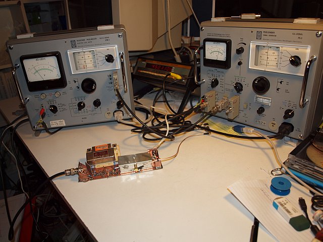
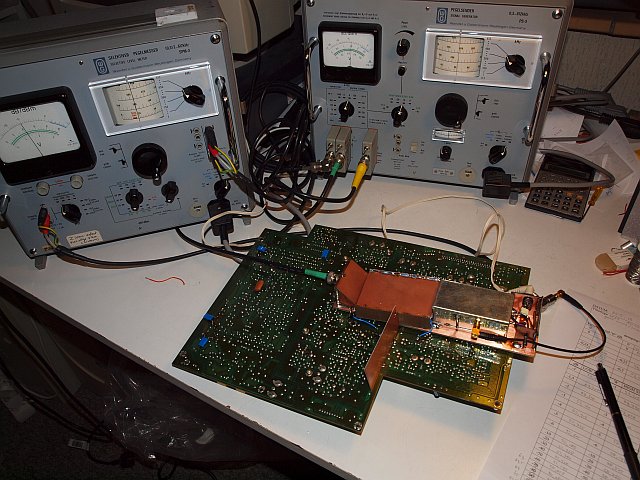
Here is the link to the page how to measure those filters and how to make additional buffer amplifiers to connect the test-setup to a Selective Level Meter. (Done with SPM-3 with PS-3 from Wandel und Goltermann, my new SPM-30 + PSE-30 will also do the job !)
Here you see a quick preview of the setup.
After all those measurements it was bizarrely clear to me why this bad CFL-230 YF455DPB JRC filter was suddenly no longer available for the successors of the NRD-515 !!!
After almost 100 measurements and the 4th build of the measuring module, the effects of HF
leakage around a filter became very clear.
The effects are a.o. a too high bottom line and very straight, no curls or strong dips. Wait a
minute, that's the same as the mainboard curves of the AM filter above!! So there is something
not quite good in the circuit! After many tests it became clear that they should have used
screened 330 uH and 4.7 mH coils. If you screen them now (with cut in half electrolytes as
caps!) the L value and Q drop too much. They should have made it the same as the SSB filter,
with screened transformers.
The difference is at least 20 to 30 dB!!
The small 14 mm 3E25 toroid Z-adapt solution I made for the Kenwood crystal filter is tested in the
setup module and later in a NRD-515 before and after the 6 kHz AM filter, in place of 330uH,
220pF and the 4.7mH. So used two times. It gave 15 - 20 dB improvement. With an additional
(still needed) screening bracket it even became 20 - 30 dB improvement!
Bad circuit is also used in other receivers, I've seen it used (in the diagrams) in the NRD-505, NRD-515, NRD-525, NRD-535, JST-125, JST135, JST-145/245.
Even Eska used it. I doubt if they used screened coils..... YES, THEY DID USE SCREENING!
tested:
Max. -65dB is hardly possible with "open" unscreened coils.
But with screened coils (a.o. with cut in half electrolytes!) and a fully screened setup I reached even under -100dB, so perfect is possible.
Tested with open 330uH Neosid coils (image): the aluminum cap reduces the L from 330uH to about 220uH, the Q drops from 45 to 16. So a coil with ferrite cap and additional screening is best... Like the coils around the Kokusai filters.
I wonder how others build it..... Screened? Or NOT?
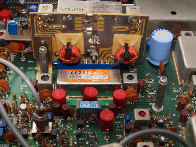
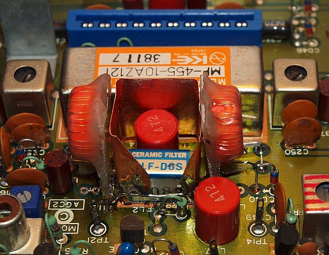
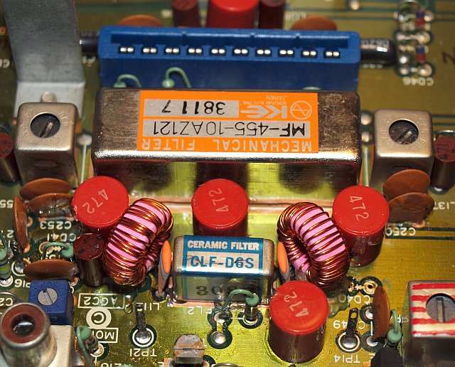
The CLF-D6S original (brown) and with toroid modification transformer 3E25 = green, 330uH 4A11 toroid = red
Test setup of the screened LC networks.
Very, very bad results without the caps!
Even with a 90 degree angle!
Image: Open coil test setup
Here (like above) how the Z-adapt toroids were used near the Kenwood filter.
Around the CLF-D6S it is still original.
View the NRD-515 mutilation with the transformer toroids. Image: Transformer test setup
I'm not the first who found this design flaw with coil leakage around an IF filter. It has been mentioned earlier by Dallas Lankford. His proposal was to replace the 330 uH coils with coils on FT50-43 toroids. A toroid is well screened by design. But mind the 3x 90 degree non interfering position. (it can be improved still! I did with the transformer screening bracket! That's the thinner blue line in the above curves.)
Dallas Lankford's testing documents are hidden now on the net - not available anymore - secret?? Or do you have to pay?? I got a stolen version. Download it before they prosecute me.
I've also tested the toroid coils intensely, as well as in a test setup, as in the NRD-515 itself. See pictures.
Now I used a toroid with a much lower AL value, chosen is 4A11 - 13 mm (TN13/7.5/5), average AL = 360. Windings number is 31, 32 or 33 (measure!) With higher AL value the losses are higher and you have a greater L step by winding. Lower is better and more accurate.
Amidon - Fair-Rite FT50-43 were unavailable at the moment. Ferroxcube 4A11 is comparable, old color = pink.
During testing under 100 kHz (LC-resonance measurement setup with 10 nF in the ferrite-toroid setup module) the original 330 uH coils have at resonance at about 88 kHz a Q of about 80 - 85, the blue 330 uH Neosid testsetup coils about 45, the small 4A11 toroid is about 40 and the FT50-43 toroid is disappointing bad, about 6 to 7. The Fair-Rite core is therefore NOT adviced by me, it has much too high losses!
I recently tested a 4C65 TN14/9/5 from Ferroxcube with my Mastech LCR. 4C65 is comparable with FT50-61. Measured AL with N=10 was a little lower as expected, 47 where it should be 55. I calculated 330uH N= +/- 85. I got my 330 uH and a Q of about 120 with my Mastech LCR set on 100 kHz.
You DO NEED a tiny fishermans winding tool made from PCB scrap to hold the wire like these ones. Test wire lenght for N = 5 and calculate total wire length for N + 5%. Tool lenght for these tiny toroids is 10 to 15 cm, width is max. 5 mm!!!
Later I also tested on the LCR a few proven OK TN13/7.5/5 4A11 toroids and a new shipment of FT50A-43 to compare them.
The list:
material
type
meas. AL
N-330u
Q
4C65
TN14/9/5
47
85
120
61
FT50A
75
65
86
4A11
TN13/7.5/5
290
33
47
43
FT50
413
25
36
old 43
FT50
770
21
6
3F3
TN13/7.5/5
970
18
45
It is also possible that my deviant old -43 (bad FT50-43) toroids are from an earlier production date. I found this on the (former) site of Clifton Laboratories. One has the "formula" of the composition of "43" sometimes adjusted (perhaps copied the composition "formula" from Philips?)! See my ferrite toroid-test and measurement story over Here.
It must therefore have been known by them that it was not perfect at all in the past.
Update: Meanwhile Clifton Laboratories removed this document from their site and is also taken over by DX Engineering .....
But HERE I have a copy on my server!!
The 2x 330uH coil in toroid shape gives easier a stable result compared with the transformer version above, 30 dB improvement is also possible. You don't have to ruin so much..... It can again be improved by 5 dB more with an additional shielding bracket (the thinner blue line in the above curves), but is not needed.
Test setup of the 4A11 toroid networks.
In the copper foil: two cascaded Murata's.
Very good results without any coil cap! Also here: at right (square) angles to each other.
Here the test setup of the filters on the Rx board. Do you dare to do that??? I added additional screening!
Less NRD-515 mutilation with 2x the 330uH 4A11 toroids. This works great with minor destruction. Mind the 90 degree angle!
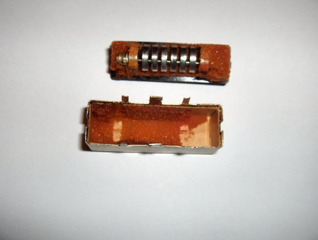
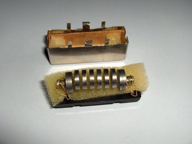
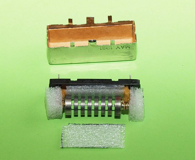
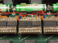
Kokusai Filter Repair:
Kokusai Mechanical filters have a habit of deteriorating in time due to decomposing of the foam inside it.
It becomes a sticky gummy mess, which dampens the vibrations of the resonating disks.
With extreme care the shit can be dissolved with nail polish remover (in Dutch: aceton) or even better with isopropyl alcohol and repaired with fresh foam. After some experience: packing foam works better than cotton wool!!
After a whole series of cleaning actions a friend of mine (PD0SDQ - Peter) developed an even better method of restoration. NO cotton wool, as I did like John, but packing foam. Almost the same as on the pictures from Luuk. But square stiffer foam blocks with a hole in it over the piezo units, that is used at the ends to position the disks only, no pressure on the disks themselves. On top and underneath only a thin sheet of foam to fill-up. Indeed it works just a bit better, lesser damping of the resonating disks!
Here you see what should be trick!!
One filter is a 2.4 kHz version, the other is a 600 Hz version. Do you notice the differences in disk numbers and the size of them??
PDF with frequency calibration notes for the NRD-515
PDF with example design (ref 4) of a frequency counter reference Droitwich PLL unit PDF with design revision no 5 of the Droitwich PLL
VLF ADDON, extension down to 10kHz:
More modifications are needed to the input circuits to work properly PDF with VLF mixer add-on (the extended version drawing)
PDF with VLF modification simple (overview sketch)
Excellent reception from about 25 kHz Only exchange some capacitors and two resistor like inductors
PDF with VLF modification extended (overview sketch)
Reception possible from about 10 kHz.
Only do this if you are very experienced, besides the adding of much larger capacitors over the existing ones, replacing a DC bypass inductor, also a relay is added and an extra input toroid in the first mixer to extend the Rx range to as low as 10 kHz without much degradation of sensitivity
See the two pictures added right.
And here you see the extended mutilation.
A copy of the low-pass, the relay and the extra mixer input toroid.
Some more additional details, not present in the PDFs above.
a) VLF simple, Rx OK from 25 kHz:
Position C15, C17, C150, add underneath a 1uF cap over the existing 100nF.
C15 should be at least 100V, better is 250V. I've seen C15 blown after tampering with the input protection diodes.
Add 0.56 uF over C16 and C25.
L7 and L11 should be replaced with at least 2.2 mH, better is 4.7 mH.
Possible use the same resistor like coils.
A toroid is better screened and is preferred for L7. Also for L11 in simple VLF change.
For about 5mH you get:
For 14mm 3E25, measured 10 kHz AL = 2240. N = 47 - 50.
For 14mm 3C11, little better Q, measured AL = 1900. N = 51 - 55.
For 12.5 mm FT50(A)-77, AL = 1100 - 1200, N= 67 - 70
b) VLF extended with extra mixer 14 to 26 mm 3E25 input toroid. 35 years ago a cheap blue 3E2 was used. There are much better toroids now, a 3E25 is better, or 3C11. Or double hight, use two 14mm on top of each other.
Original measured toroid voltage level is 1 : 3.6. Z probably 50 : 640 Ohm. To calculate N, primary Z-coil = 4 x 50 Ohm = 200 Ohm Z, L = 3.2 mH, secondairy 640 Ohm = 2x 2550 Ohm Z, L= 2x 41 mH. Use twisted bifilar wire. N = 1000 sqrt( mH / AL).
The needed 2.2 uF cap's are mostly to big for C15 and C17 position. I replaced 100 nF with one 1uF and an extra 1uF underneath. C150 is not needed to change.
L11 and CD2 are not used, one leg is "lifted".
L7 is as above.
PHOTOGRAPHS section:
Photographs from the NDH-518 memory unit with eprom BIN-BCD address decoder, push-button and rotary-opto up-down control Click here or on picture for sub-page
Photographs from the NDH-515 memory unit with two GAL's for BIN-BCD decoding. Only one hole for extra bankswitch needed Click here or on picture for sub-page
Photographs from the NDH-518 memory unit with two GAL's and remote control options. Most complex version Click here or on picture for sub-page
The design of a set of replacement uPD5101 modules for an exploded memorybank NEW In DUTCH and ENGLISH available Click here or on picture for sub-page
Photographs from the NWG-515 Remote VFO A NWG-515 ?!?, a very peculiar thing.
Click here or on picture for sub-page
Mains-inlet changes Safety modifications mains filter to comply with new regulations IEC power input exchange with real mains-inlet filter. Click here or on picture for sub-page
Click over HERE for a direct hop over to all the other radio information on the next page.
If you do not have the "Acrobat Reader", please access to the site of Adobe Systems Incorporated. The Acrobat Reader is distributed by Adobe
Systems Incorporated free of charge. Adobe, Acrobat Reader, and their logo marks are registered
trademarks of Adobe Systems Incorporated.
A nice NRD-515 YouTube video I found,
a perfect place over here to embed it.
And there is a lot more to see...

 NRD-515 oriented

 installed, see at the bottom of this page.