Problem statement and the subsequent dissolving design stages.
Got - a gift!: JRC memory unit NDH-518, blown after a lightning strike and spark-over at the JRC unit.
The spark mark spot (on a screw) is still visible.
On the inside no visible trace damage on the board, but a lot of semiconductors are "exit". (What about the receiver damage......) In particular the (ancient) memory IC's. Yet sin to demolish, repair perhaps? Designing an interface for modern and inexpensive IC's with 32,768 channels? A trial version is already working! But is a little "overkill"!
All TTL and CMOS is cheap and easy to replace, a little harder is the old memory IC MCM5101 or uPD5101 in super low power version (with -LL in the serial number).
The 5101 is really antique, with a total of only 1024 bits in 256-nibble slices of 4 bits. And also with separate input and output for the databits! 256 million bits per chip is actually even antique also nowadays.
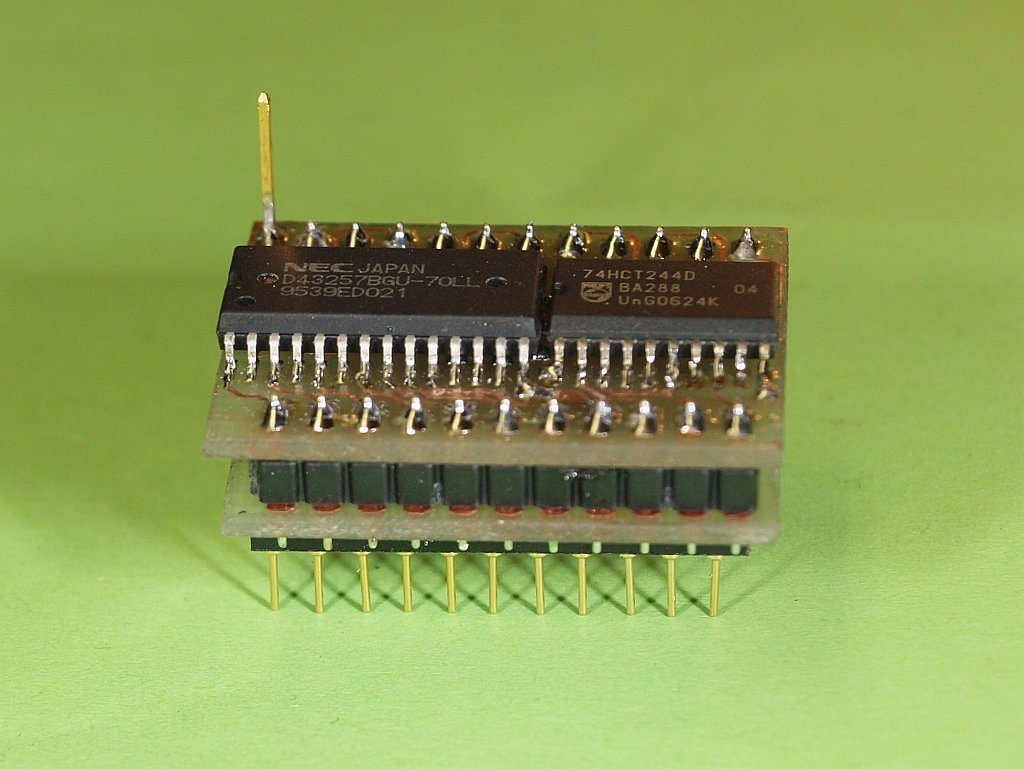
A sheer lucky coincidence: on the radio fleamarket in Rosmalen (NL), I ran across a cheap tube of uPD43257BGU-70LL in SMD, in effect to at least 250x greater memory capacity, a complete different kind of CMOS static RAM chip. But with "-LL", superlowpower, suitable for battery-backup! And maybe applicable in an appropriate interface circuit in a small PCB-module with a 22 pin "IC plug". But everything will have to stay super compact to fit!
It would be nice having the entire interfacing also on this tiny board, so that (almost) nothing has to be changed or "cut" at the original JRC board. It shouldn't become much larger in length than the original IC, in the width direction some extra "stretch" is possible.
After some thought-noise a thought has been put on paper. Would it work? How much current would it consume? Will the data I/O interfacing work at Vbatt, or must it due of it's current use be separated and connected to the standard +5V Vcc? To separate is still better, so an extra pin to Vcc is needed unfortunately.
PDF link First (error) version.
To ease "wiring" on the tiny board: all data and address bits are jumbled, it makes no difference. Don't be worried.
It is recommended building a testcircuit and verify it all, preferably with applying the original SMD components. Where do I obtain an appropriate SMD experiment board? Is rare, or not for sale. OK, then I also design that myself. PDF link to a 10 x 16 cm euro SMD experimental board, type PE1ABR!
Another weekend nicely busy with UV exposing, etchings and soldering on a scrap piece of the euro-SMD board.
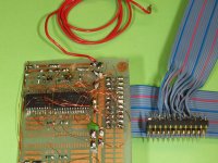 After another weekend busy with monkeyhair copper wire (<0.1 mm!) and SMD grit: it works. Current consumption is much too high. More than 60 uA. Standby time only half a year with one set of batteries? Can't be OK, there's an IC leak or something is not right there. Address-bit leak: can not be. After examination of the pull-down on the data I/O signals: that's not either a problem.
It turns out to be an external /WE pull-up of 47K connected to Vbatt. Probably is a MEM write protect security at on/off, by keeping signal /WE constant high to Vbatt. The pull-up power is leaking away through the buffer interface via the input protection diodes if the buffer is powerless and Vbatt is present. In short: directly to /WE NO standard inverter transistor nor a HC(T) gate with protection-diodes (in forward conduction) will work, only with real isolated gate inverters or reverse connected diode protection buffers are applicable. Well we use a stage with two BSN type FET's, an isolated gate buffer to connect signals to the data interface. Again a modified sketch:
PDF link schematic version 2, the improved version. After another weekend busy with monkeyhair copper wire (<0.1 mm!) and SMD grit: it works. Current consumption is much too high. More than 60 uA. Standby time only half a year with one set of batteries? Can't be OK, there's an IC leak or something is not right there. Address-bit leak: can not be. After examination of the pull-down on the data I/O signals: that's not either a problem.
It turns out to be an external /WE pull-up of 47K connected to Vbatt. Probably is a MEM write protect security at on/off, by keeping signal /WE constant high to Vbatt. The pull-up power is leaking away through the buffer interface via the input protection diodes if the buffer is powerless and Vbatt is present. In short: directly to /WE NO standard inverter transistor nor a HC(T) gate with protection-diodes (in forward conduction) will work, only with real isolated gate inverters or reverse connected diode protection buffers are applicable. Well we use a stage with two BSN type FET's, an isolated gate buffer to connect signals to the data interface. Again a modified sketch:
PDF link schematic version 2, the improved version.
Test... It doesn't work? There is absolutely no current use?? But it does work!
Well, well, it works so well now (with super low power consumption in "sleep" mode) that I even doubt whether the IC is connected to the power supply. Less than 1 uA use, least significant bit on the digital current indicator flashes only! 1 uA resolution is the lowest of my meter. Vbatt and Vcc connected together is now no longer possible, as always 1 of the two inverter FET's draws current (> 200 uA).
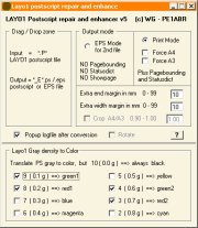
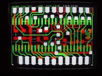 Testing in trial-mode is successful now, the lay-out work can start on the real PCB. Would It be possible to get it all on the tiny board? Quickly enjoyed many hours with good old-Layo1 for DOS. I like to have an old W98-special occasion up and running with a simple VESA video card, so nostalgic DOS VESA Video programming commands work OK. And it looks fine and works perfectly, and I can handle it. In order to continue using the old Layo1 I have more reasons. The key: the output files generated by Layo1 themselves
in postscript (only this version) are of a very clear and easy to understand structure. I can break-in in those files later to get beautiful conversions out of it! I.E. with my own conversion software I can generate and convert from the graystairs output from the Layo1 outputdriver to color and also "clean" the postscript so I become flawless production sheets and perfect documentation in color without strange errors when converting the postscript to PDF format.
Testing in trial-mode is successful now, the lay-out work can start on the real PCB. Would It be possible to get it all on the tiny board? Quickly enjoyed many hours with good old-Layo1 for DOS. I like to have an old W98-special occasion up and running with a simple VESA video card, so nostalgic DOS VESA Video programming commands work OK. And it looks fine and works perfectly, and I can handle it. In order to continue using the old Layo1 I have more reasons. The key: the output files generated by Layo1 themselves
in postscript (only this version) are of a very clear and easy to understand structure. I can break-in in those files later to get beautiful conversions out of it! I.E. with my own conversion software I can generate and convert from the graystairs output from the Layo1 outputdriver to color and also "clean" the postscript so I become flawless production sheets and perfect documentation in color without strange errors when converting the postscript to PDF format.
A quick SMD PCB view??
 Also you can use my software to convert the standard output of layer 1 and 2 not only to a cleaned postscript but also adjusted to the EPS file format. Later you can then merge (by hand) several small postscript jobs in Notepad+ and still use only 1 printsheet,
or make macros in postscript to make multiple (identical) print jobs on the same sheet.
Also you can use my software to convert the standard output of layer 1 and 2 not only to a cleaned postscript but also adjusted to the EPS file format. Later you can then merge (by hand) several small postscript jobs in Notepad+ and still use only 1 printsheet,
or make macros in postscript to make multiple (identical) print jobs on the same sheet.
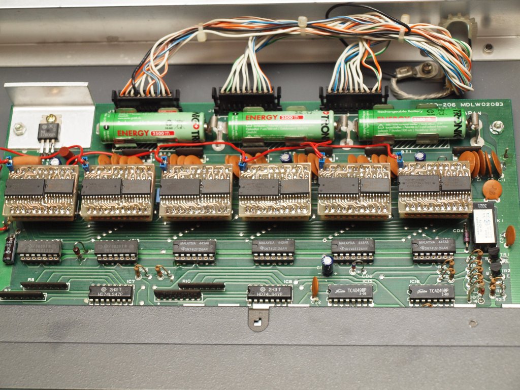
PDF link of 10 mini-memory IC PCB-boards in 2 handprogrammed sheets (1 sheet per layer).
Pleasant economical and enormous useful for the same small PCB (again as in this case) when you need a large number of them.
After generating a PDF from the "cleaned" postscript you see how it looks, and is subsequently also easier to print from Acrobat on a different (modern) PC with all modern printer options. With the tiny memory PCB and etching them at home the chance to create more waste is unfortunately bigger.
|